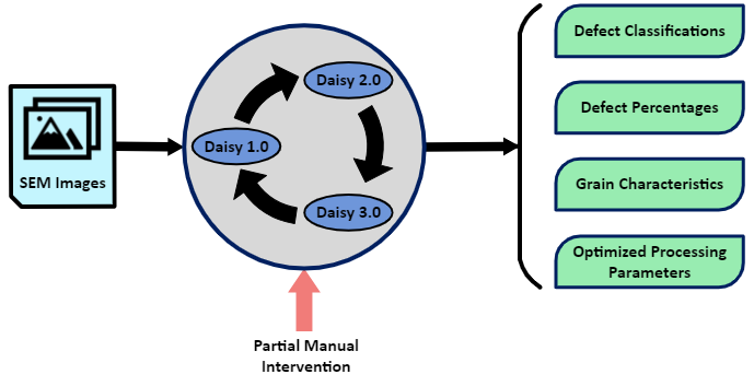
Daisy Workflow for SEM image characterization
Thin films are crucial in technologies such as photovoltaics, semiconductors, and coatings, making their quality vital for performance. Scanning Electron Microscopy (SEM) aids in analyzing these films, but manual image analysis is labor-intensive and error-prone. The Daisy project aims to develop a computer vision and machine learning workflow to automate defect detection and grain analysis in thin film SEM images. This workflow will implement segmentation, classification, and clustering models, including the Segment Anything Model (SAM), to detect and quantify defects. Additionally, it will measure and analyze grain size and distribution.
The data obtained will optimize processing parameters using state-of-the-art machine learning techniques, helping to identify key manufacturing and material parameters for optimal thin film fabrication. Methodologies include applying transfer learning to adapt pre-trained models for defect detection, fine-tuning models to distinguish between grains and defects, using clustering algorithms for classification, automating data labeling and management, and analyzing data to extract meaningful feature importances. This software will optimize thin-film manufacturing by automating defect detection and improving grain characterization, significantly reducing analysis time and effort, and thereby enhancing research and development in thin-film technologies.